- 您现在的位置:买卖IC网 > Sheet目录1904 > AT91SAM9G20B-CFU (Atmel)IC MCU ARM9 247-LFBGA
5
6384DS–ATARM–13-Jan-10
AT91SAM9G20 Summary
3.
Signal Description
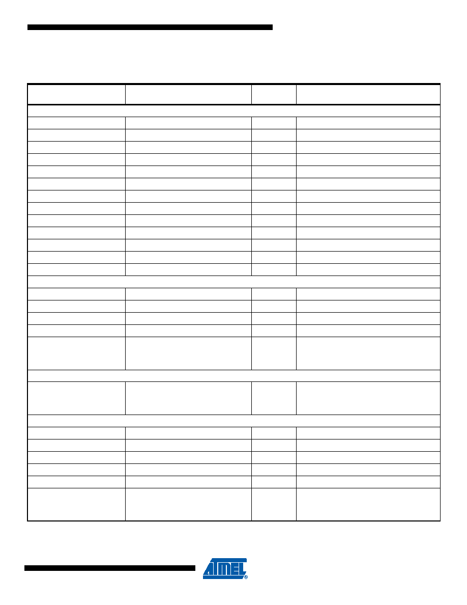
Table 3-1.
Signal Description List (Continued)
Signal Name
Function
Type
Active
Level
Comments
Power Supplies
VDDIOM
EBI I/O Lines Power Supply
Power
1.65V to 1.95V or 3.0V to 3.6V
VDDIOP
Peripherals I/O Lines Power Supply
Power
1.65V to 3.6V
VDDBU
Backup I/O Lines Power Supply
Power
0.9V to 1.1V
VDDANA
Analog Power Supply
Power
3.0V to 3.6V
VDDPLL
PLL Power Supply
Power
0.9V to 1.1V
VDDOSC
Oscillator Power Supply
Power
1.65V to 3.6V
VDDCORE
Core Chip Power Supply
Power
0.9V to 1.1V
VDDUSB
USB Power Supply
Power
1.65V to 3.6V
GND
Ground
GNDANA
Analog Ground
Ground
GNDBU
Backup Ground
Ground
GNDUSB
USB Ground
Ground
GNDPLL
PLL Ground
Ground
Clocks, Oscillators and PLLs
XIN
Main Oscillator Input
Input
XOUT
Main Oscillator Output
Output
XIN32
Slow Clock Oscillator Input
Input
XOUT32
Slow Clock Oscillator Output
Output
OSCSEL
Slow Clock Oscillator Selection
Input
Accepts between 0V and
VDDBU.
PCK0 - PCK1
Programmable Clock Output
Output
Shutdown, Wakeup Logic
SHDN
Shutdown Control
Output
WKUP
Wake-up Input
Input
Accepts between 0V and
VDDBU.
ICE and JTAG
NTRST
Test Reset Signal
Input
Low
Pull-up resistor
TCK
Test Clock
Input
No pull-up resistor
TDI
Test Data In
Input
No pull-up resistor
TDO
Test Data Out
Output
TMS
Test Mode Select
Input
No pull-up resistor
JTAGSEL
JTAG Selection
Input
Pull-down resistor. Accepts
between 0V and VDDBU.
RTCK
Return Test Clock
Output
发布紧急采购,3分钟左右您将得到回复。
相关PDF资料
AT91SAM9N12-CU
IC MCU ARM9 217-LFBGA
AT91SAM9R64-CU-999
IC MCU ARM9 32KB ROM 144LFBGA
AT91SAM9XE512-QU
MCU ARM9 512K FLASH 208-PQFP
AT97SC3204-X1A50-1
CRYPTO TPM LPC 3.0-3.6V 28TSSOP
ATA6620N-TAQY
TXRX LIN BUS W/VREG SO-8
ATA6661-TAQJ 19
TXRX LIN 2.0 3.3V/5V 8SOIC
ATA6670-FFQW
IC TXRX LIN DUAL 14VDFN
ATAM893T-TKSYD
IC MCU FLASH 4K MTP 20SSOP
相关代理商/技术参数
AT91SAM9G20B-CU
功能描述:ARM微控制器 - MCU 2x16K SRAM Ethernet USB Host Bus Intrfc
RoHS:否 制造商:STMicroelectronics 核心:ARM Cortex M4F 处理器系列:STM32F373xx 数据总线宽度:32 bit 最大时钟频率:72 MHz 程序存储器大小:256 KB 数据 RAM 大小:32 KB 片上 ADC:Yes 工作电源电压:1.65 V to 3.6 V, 2 V to 3.6 V, 2.2 V to 3.6 V 工作温度范围:- 40 C to + 85 C 封装 / 箱体:LQFP-48 安装风格:SMD/SMT
AT91SAM9G20B-CU-999
功能描述:ARM微控制器 - MCU 2x16K SRAM Ethernet USB Host Bus Intrfc RoHS:否 制造商:STMicroelectronics 核心:ARM Cortex M4F 处理器系列:STM32F373xx 数据总线宽度:32 bit 最大时钟频率:72 MHz 程序存储器大小:256 KB 数据 RAM 大小:32 KB 片上 ADC:Yes 工作电源电压:1.65 V to 3.6 V, 2 V to 3.6 V, 2.2 V to 3.6 V 工作温度范围:- 40 C to + 85 C 封装 / 箱体:LQFP-48 安装风格:SMD/SMT
AT91SAM9G20-CU
功能描述:ARM微控制器 - MCU 32-bit
RoHS:否 制造商:STMicroelectronics 核心:ARM Cortex M4F 处理器系列:STM32F373xx 数据总线宽度:32 bit 最大时钟频率:72 MHz 程序存储器大小:256 KB 数据 RAM 大小:32 KB 片上 ADC:Yes 工作电源电压:1.65 V to 3.6 V, 2 V to 3.6 V, 2.2 V to 3.6 V 工作温度范围:- 40 C to + 85 C 封装 / 箱体:LQFP-48 安装风格:SMD/SMT
AT91SAM9G20-EK
功能描述:开发板和工具包 - ARM 32-bit MCU Eval Kit
RoHS:否 制造商:Arduino 产品:Development Boards 工具用于评估:ATSAM3X8EA-AU 核心:ARM Cortex M3 接口类型:DAC, ICSP, JTAG, UART, USB 工作电源电压:3.3 V
AT91SAM9G25-BFU
制造商:Atmel Corporation 功能描述:VFBGA, GREEN, IND TEMP, MRLA - Trays 制造商:Atmel Corporation 功能描述:IC MCU ARM9 64KB ROM 247VFBGA
AT91SAM9G25-BFU-999
制造商:Atmel Corporation 功能描述:VFBGA,GREEN,IND TEMP,MRLA,T&R - Tape and Reel 制造商:Atmel Corporation 功能描述:IC MCU ARM9 64KB ROM 247VFBGA
AT91SAM9G25-CFU
功能描述:微处理器 - MPU TFBGA GRN IND TEMP MRLA
RoHS:否 制造商:Atmel 处理器系列:SAMA5D31 核心:ARM Cortex A5 数据总线宽度:32 bit 最大时钟频率:536 MHz 程序存储器大小:32 KB 数据 RAM 大小:128 KB 接口类型:CAN, Ethernet, LIN, SPI,TWI, UART, USB 工作电源电压:1.8 V to 3.3 V 最大工作温度:+ 85 C 安装风格:SMD/SMT 封装 / 箱体:FBGA-324
AT91SAM9G25-CFU-999
制造商:Atmel Corporation 功能描述:BGA,GREEN,IND TEMP,MRL A,T&R 制造商:Atmel Corporation 功能描述:BGA,GREEN,IND TEMP,MRL A,T&R - Tape and Reel 制造商:Atmel Corporation 功能描述:IC MCU ARM9 ROM 247BGA 制造商:Atmel Corporation 功能描述:BGAGREEN,IND TEMP,MRL A